
PCB Glossary
ATE : Automatic Test Equipment
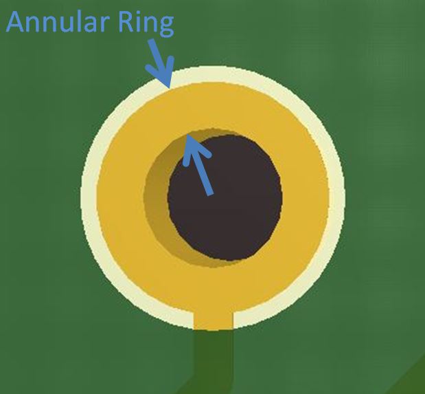
Annular Ring : The copper land that surrounds a drilled hole on a layer that is required to make an electrical connection with another part of the circuit. The fabricator will specify a minimum annular ring requirement based on the design technology. Factors that affect the size of the annular ring include the board thickness, number of layers and drill size.
BBT : Bare Board Test – Test performed on the bare board (un-populated) by the PCB fabricator against the design data netlist to ensure that the finished board agrees with the original data. This can be performed using a bed-of-nails or a flying probe tester.
Aspect Ratio : The aspect ration of a design is the thickness of a PCB divided by the smallest mechanically drilled hole. Manufacturer’s will state the achievable aspect ratio, such as 10:1 or 8:1, for a specific design technology. The higher the aspect ratio the more difficult the board will be to fabricate and as such will increase cost.
BGA : Ball Grid Array – Integrated circuit package whose pins are formed as balls on the bottom of the device. The pins may be placed either as a fully populated array or as a courtyard pattern. Because the pins are placed in an array they are normally numbered using an alpha-numeric scheme, with the numbers and letters corresponding to rows and columns. BGA pin pitches are normally 1.0mm – 0.8mm. Some older devices do have pin pitches of 1.27mm.
Blind Via : A via that has a connection that starts on an outer-layer of a PCB and stops on a predefined internal layer. The vias can be created in a number of ways using a number of build-up technology approaches or by creating PCB sub-assemblies.
Buried Via : A via that has a connection that starts on one internal layer of a PCB and stops on another predefined internal layer. The vias can be created in a number of ways using a number of build-up technology approaches or by creating PCB sub-assemblies.
Courtyard pattern: Related to BGA pin patterns; a courtyard pattern is when an area of the pin array is not populated with balls so that this forms a square which resembles a courtyard. The area may be the complete middle section or it can be a moat area – pins placed in the middle of the device followed by a gap, then more pins towards the edge.
CSP: Chip Scale Package – Integrated circuit package similar to a BGA. What distinguishes the CSP from the BGA is that the package size is no greater than 20% of the bare die size.
Die: The semiconductor substrate containing the integrated circuit.
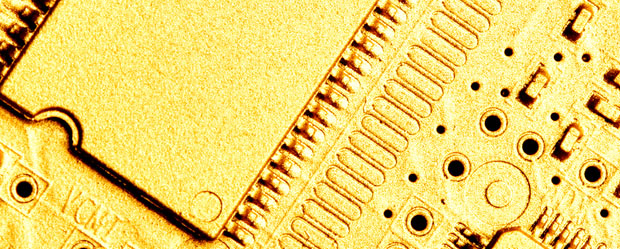
PCB etching: : what is it? PCB etching involves removing unwanted copper from printed circuit boards. When the excess copper from the PCB has been removed, only the circuit required remains. The layout of the board is generated before the etching process begins.
EMC: Electromagnetic compatibility understanding and management of unintentional creation, propagation and reception of electromagnetic energy which may cause unwanted effects such as electromagnetic interference (EMI) or even physical damage in operational equipment.
Finished Drill Hole Size: The size of hole that you want the board to be delivered with. Fabricators will drill the hole larger than the finished hole size to allow for the thickness of the plating which will be added during the fabrication process to create a connection between the top, inner layers and bottom surfaces of the hole. The drilled hole size should be taken into account when calculating the annular ring.
Functional Testing: A test performed on a populated PCB at the end of the manufacturing process to determine if the product performs to specification and can be shipped. The board is automatically subjected to a pre-defined set of test vectors /stimulus with the results determining whether the design passes or fails.
Gap: One part of a term widely used in the industry, “track and gap”, the gap is the dimension or clearance between two traces on a PCB. The desired gap can vary dependent on the design parameters such as voltages, crosstalk and other electrical considerations. The fabricator will also specify a minimum gap for maufacturing purposes on your design.
Guide: This is the term used by some CAD systems for an element that graphically shows the connection between component pins. As the designer adds the copper connections to the design the guides generally disappear to show that the connection is complete. They are also know as fromtos and rats tails or rats nest.
Gull Wing: A type of surface mount lead formation where the component lead is bent in such a way as to resemble the letter S or a gull wing. The corresponding copper pad connection is external to the component body. This lead formation is found on variety of devices such as SOICs and QFPs.
ICT: In-Circuit Testing – Test performed on a populated PCB where an electrical probe is used to check the board for errors such as shorts, opens and missing components. A bed-of-nails or a flying probe can be used to run the checks.
Impedance extends the concept of electrical resistance in alternating current (AC) circuits, and unlike resistance that has only one possesses both magnitude and phase, unlike resistance, which has only magnitude, impedance is measured in a time-varying and voltage-varying Impedance could be classed as the overall resistance of ALL the components in a given circuit.
LCC: Leadless Chip Carrier – Integrated circuit surface mount package that has pins on all 4 sides of the device. The leads are an integral part of the device with the pins being embedded vertically within the component body equally spaced along the edges.
Looping: What is a PCB ground loop? – Ground loops occur when the ground potentials differ in different parts of the circuit, causing multiple paths of current return. This results in the current flowing through paths that are shorter than the desired route. On a PCB assembly, all the ground planes and points should have the same potential.
LGA: Land Grid Array – The LGA is similar to a BGA package in terms of pin placement across the package; however rather that use balls to provide the connection to the PCB it has flat metal pads on the bottom of the device.
Microcontroller (MCU) – A microcontroller controls a single function in a device inside a system. On a typical microcontroller, there are a processor (CPU), memory, and input/output (I/O) peripherals. The central processor interprets data it gets from I/O peripherals. The microcontroller stores the temporary information it receives in its data memory, where the processor uses instructions in its program memory to decode and apply it. A peripheral uses I/O to communicate and perform the action.
Micro-Via: A micro-via also, known as a uVia or µVia, is an extremely small via, 0.15mm (~6thou) or smaller, that is usually laser drilled. The size of the hole is generally governed by the thickness of the dielectric layer that the laser will have to cut through. The vias are commonly used in dense PCB designs.
Mycelium
A mycelium is a network of fungal threads or hyphae. The fruiting bodies of fungi, such as mushrooms (see Computer Mushrooms article), can sprout from a mycelium. usually grows underground it also thrives in other places such as rotting tree trunks. A single spore can develop into a mycelium.
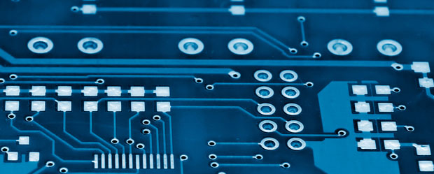
PCB: Printed Circuit Board – The PCB is a laminated structure that provides the electrical connections between components that are mounted on the board. The connections or tracks are etched from copper clad layers that are then bonded together using heat and pressure. Connections between the layers are created by drilling holes through the board and then plating the holes with copper; these structures are known as vias.
PLCC: Plastic Leaded Chip Carrier – Rectangular Integrated circuit surface mount package that has pins on all 4 sides of the device. The leads are normal J-shaped, bent underneath the body of the device.
Power Connectors: Board-to-board (BTB) connector – Used to connect PCB’s (printed circuit boards) (PCB), electronic components in an reliable and repeatable manner.The terminal is made from a conductive material and housed in insulating material to protect from inteference. Terminals transmit the current/signal between PCBs through the connector and so termed BTB.
wire-to-edge power connector
Printed Circuit Technology:
printed Liquid Crystal Polymer
PWB: Printed Wiring Board – See PCB
PWA: Printed Wiring Assembly – See PCB
QFP: Quad Flat Pack – Rectangular Integrated circuit surface mount package that has pins on all 4 sides of the device with its leads formed as gull wing.
SOIC: Small Outline Integrated Circuit – Rectangular Integrated circuit surface mount package that has pins on 2 sides of the device which are formed using the Gull-Wing pattern. The standard pin pitch for a SOIC is 1.27mm/50thou – half that of a standard DIP. The SOIC was the natural replacement for the older DIP (through hole technology) style package and they normally have the same pin-outs as their counterpart DIP devices. There are a number of SOIC package styles such as Wide and Narrow.
SOP: Small Outline Package – Rectangular Integrated circuit surface mount package that has pins on 2 sides of the device that are formed using the Gull-Wing pattern. The standard pin pitch for a SOP is 1.27mm/50thou.
Stackup: The definition of the PCB construction including the number of layers, copper weight (thickness), together with the material type and thickness of the dielectric layers that separate and therefore electrically insulating the copper layers from each other; the stackup will also stipulate the final PCB overall thickness. The design of the stackup is a critical factor in defining the board’s performance and should be carried out with the fabricator.
Track/Trace: The name given to the copper that connects two or more component pins together. The width of the copper track depends upon many factors, including the components used, the signal’s electrical requirements and the current that the trace will have to carry. The fabricators will also stipulate a minimum track size depending upon the technology of the design.
TSOP: Thin Small Outline Package – Rectangular Integrated circuit surface mount package that has pins on 2 sides of the device which are formed using the Gull-Wing pattern. The pin-pitch for these devices can go as low as 0.5mm/20thou. The leads are placed along the width (shortest length) of the component. These packages are very low profile, normally about 1.0mm/40thou, and are widely used in slimline applications such as memory devices for laptop computers.
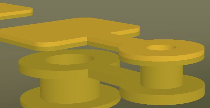
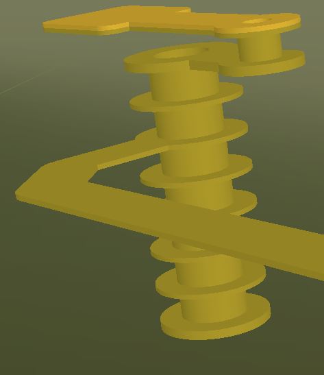
Via: A via is the way that a electrical connection or trace changes from one layer of a PCB to another. Vias are essentially a hole with a thin coating of copper applied to the barrel to provide the electrical connection. Holes can be created in a number of ways including mechanical drilling, laser drilling as well as plasma etching.