ICT Annual Symposium 6th June 2023
keynote speakers at the Institute of Circuit Technology's Annual Symposium
At the lovely National Conference Centre in the heart of the UK Midlands, Sue and Andy Critcher, the dynamic team behind the design firm Total Board Solutions, took centre stage as the keynote speakers at the Institute of Circuit Technology’s Annual Symposium.
Technical director Bill Wilkie welcomed everyone to the event and provided interesting commentary on the changing UK PCB market to get things started. He emphasised the Institute’s flexibility and dedication to staying on the cutting edge.
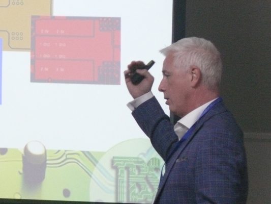
With their abundance of knowledge, Sue and Andy Critcher fascinated the audience with their presentation on the most recent design specifications for board fabricators. They shed light on the difficulties PCB designers encounter in the quick-paced world of today, including the constant compression of component dimensions and the mounting strain of shortened project timelines. They emphasised the significance of choosing the appropriate data format and nailing the stackup specification in order to produce correct documentation. Additionally, Andy Critcher explored the subtleties of CAD-CAM tests and offered insightful information on the variations between different CAD systems.
The future of PCB design and the critical requirement for knowledge transfer to the next generation of engineers were other topics Sue Critcher spoke on that were important to the industry. Many others have the same worries, thus she emphasised the significance of developing fresh talent and facilitating an easy transfer of knowledge.
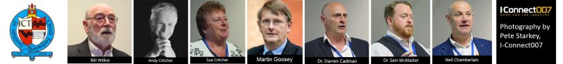
Neil Chamberlain from Polar Instruments presented the paper “Impedance and Beyond,” which contained his knowledge gleaned from an unlikely source—an eye-opening experience while carrying out a significant home renovation. Chamberlain emphasised the value of having the appropriate tools and being proficient in their effective usage by drawing comparisons between this unexpected adventure and the world of PCB design. He described Polar Instruments’ dedication to provide designers, laminate producers, and PCB fabricators a comprehensive suite of tools that includes impedance modelling, stackup design, documentation, test coupon production, and measurement.
Chamberlain addressed a number of important issues, including “Who should design the stackup?” He clarified that the response is based on various elements, including the customer, particular board needs, and the intricacy of the design. Polar has created an enormous library of materials encompassing a variety of laminates to assist designers in their endeavour. This useful tool enables designers to simulate and decide whether higher-grade materials are required or whether regular FR-4 can achieve the desired performance. Polar’s stackup tool also makes it possible to create test coupons for actual measurements of important parameters.
What loss can I anticipate for my system? was another pressing topic Chamberlain addressed. He highlighted that longer cables typically result in higher losses, regardless of the characteristic impedance, using the example of a coaxial cable. He did, however, offer a novel solution that could forecast predicted losses along the line at particular frequencies. This solver considers copper geometry, copper roughness, and material properties, giving designers helpful information for improving their designs.
Chamberlain emphasised how crucial it is for designers to be knowledgeable about these techniques and the variety of materials available in order to avoid needless over-specification, which can raise prices. He did a thorough investigation of the factors influencing loss, concentrating on the effects of copper roughness and skin effect. Fascinatingly, he emphasised that copper roughness can occasionally be more important than the laminate itself at frequencies exceeding 1 GHz. It is becoming more and more important to comprehend the placement of “smooth” and “rough” surfaces inside the stackup as well as the advantages of reverse-treated and low-profile foils.
Dr. Sam McMaster from Pillarhouse International resumed the symposium with an interesting talk that focused on the difficulties of selective soldering and the cutting-edge training options his business provides. Dr. McMaster thoroughly researched all soldering procedures, including fluxing, preheating, and soldering.
He emphasised the use of the drop-jet approach, a precise flux application method that uses less material and doesn’t require as much PCB cleaning. The ultrasonic fluxing technique, which Dr. McMaster also introduced, promises quick flux application and high solids capacity. Both approaches offer compatibility with many flux types and need little upkeep.
Preheating’s crucial significance in the selective soldering process was thoroughly explained. Dr. McMaster provided engrossing video clips demonstrating temperature monitoring during preheating, and factors including assembly thickness, thermal mass, and flux activity were taken into consideration.
In terms of soldering settings, Dr. McMaster argued that nitrogen inertion should be used to ensure acceptable flow characteristics and minimise problems like bridging and dross production. He advised keeping an upper limit of 50 ppm of oxygen for the best outcomes. A key factor in successfully soldering was highlighted as being the placement of the solder bath, which applies solder to the PCB’s underside.
The symposium served as a venue for acknowledgment as well as a centre for knowledge exchange. On the occasion of his retirement from the ICT Council, Lawson Lightfoot was honoured for his outstanding services during a special award ceremony.
Professor Martin Goosey from MTG Research also spoke at the occasion and wowed the crowd with the ReGail project. This ground-breaking project focuses on the recovery of gallium utilising novel non-aqueous methods and deep eutectic solvents from end-of-life LED lights. Gallium and indium have showed promising potential for electro-depositing and dissolving in deep-eutectic solvents, with the potential for metal separation following dissolution. The ReGail project represents a significant advance in developing a circular economy approach to gallium recovery and provides a long-term fix for this essential raw element.
The Compound Semiconductor Applications (CSA) Catapult’s Dr. Darren Cadman took the podium to discuss the enormous advantages of compound semiconductors over silicon. He passionately argued for their widespread acceptance in numerous industries by highlighting their superior electron mobility, processing speed, energy efficiency, and sensing capabilities. Dr. Cadman provided insight into the CSA Catapult’s emphasis on sub-system and system optimisation, as well as their persistent work in creating innovative tools and processes for the production of compound semiconductor products.
Dr. Cadman provided a compelling example of how compound semiconductors have the potential to revolutionise robotics, driverless vehicles, renewable energy, and telecommunications. He discussed the advantages of energy-efficient networks and the difficulties associated with thermal management and packaging, particularly when wireless cellular networks made the transition from 4G to 5G. The mention of hybrid wireless bonding and micro-bump techniques for semiconductor chip connectivity, together with the availability of cutting-edge manufacturing facilities to implement these ground-breaking technologies, piqued the audience’s interest.
The Institute wanted to offer its sincere appreciation to all of the presenters, exhibitors, and attendees for their active engagement as the symposium came to a close. The attendees were also in for a treat when they went to the motorbike museum. It was a wonderful way to close a day of learning and friendship.
We have achieved the IPC Certified Interconnect Designer (CID) qualification – this qualification is based on the leading IPC standards for PCB design and is the only formal qualification for PCB design world-wide
All TBS designers are conversant with the requirements and nuances of
- Analogue design
- Digital design
- Power Supply (LTM)
- RF – Stripline/Microstrip
- Mixed Signal design
- Microwave design
- High-power/voltage design
- High-speed design – Signal Integrity
- EMC/EMI
- Intrinsically safe operation
This diverse range of customer requirements has meant that a wide range of board construction has been considered to provide the optimum solution for each requirement. As a result we have extensive knowledge when designing using
- Single sided
- Double sided
- Multilayer
- Flex
- Flexible-rigid
- Ceramic substrates (Thickfilm/thinkfilm Hybrid design)
- Exotic materials – Polyimide, PVC etc
The board construction is just one part of the manufacturing requirement; the assembly and component mounting schemes also drive the final solution. As such we also have the required skills when dealing with
- Through hole Component
- MD Components
- BGAs, µBGAs and LGAs
- µVias, blind and buried vias
- CSPs
- Flip-chip
- Bare-die
- LGA (Land Grid Arrays)
- LTM Power Devices
Our aim is to provide the right solution to you at the right time. We pride ourselves on being able to match the right design, fabrication and assembly techniques to deliver a cost effective solution for both your prototype and production needs.
When designing any PCB we always consider the DFM (Design For Manufacture), DFA (Design For Assembly) and DFT (Design For Test) requirements as a matter of course – our strong links with both fabrication and assembly houses enable us to liaise at every step of the design process to find the correct solution ensuring a quality product.